To use this site, please disable the ad blocking feature and reload the page.
This website uses cookies to collect information about your visit for purposes such as showing you personalized ads and content, and analyzing our website traffic. By clicking “Accept all,” you will allow the use of these cookies.
Users accessing this site from EEA countries and UK are unable to view this site without your consent. We apologize for any inconvenience caused.
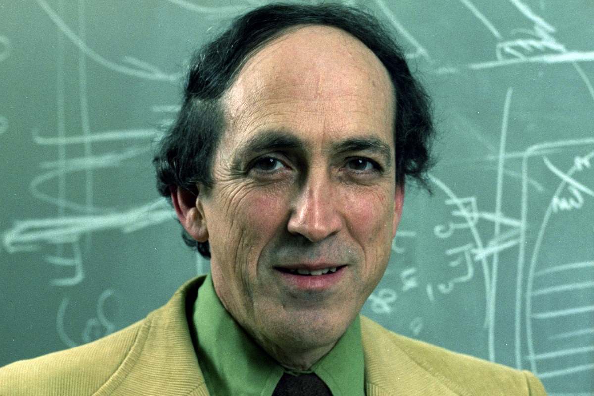
IBM research engineer Robert H. Dennard went home discouraged one evening in 1966. Another group in the company had made a presentation that showed how a system using ultrathin magnetic film for memory could boost computing power and shrink the size of the hulking mainframe machines.
Dr. Dennard worried that his team was being outpaced by focusing on silicon-based transistor technology in the race for faster and smaller computers. That night, he reworked the transistor configurations. In his notebook, he came up with an outline that would become one of the eureka moments that helped create the digital age.
His concept for a one-transistor memory cell, down from the six that were currently used, was the technological equivalent of rocket fuel. Dr. Dennard’s system, called dynamic random-access memory, or DRAM (pronounced D-ram), propelled the computing industry toward ever-smaller and more powerful systems, and led to the super-memory chips that drive the tools of modern life from smartphones to laptops to advances in artificial intelligence.
“I knew it was going to be a big thing,” recalled Dr. Dennard, who died April 23 at a hospital in Sleepy Hollow, N.Y., at 91, “but I didn’t realize how much it would grow.”
What Dr. Dennard conceived was an elegant solution to a major conundrum at the time: how to amplify computing speed and scope while trying to manage the size of the devices. By the mid-1960s, computers were playing an increasing role in areas such as industrial design, the aerospace industry and bookkeeping, but the machines were behemoths that relied on vast internal wiring and often cumbersome magnetic-based data storage.
DRAM offered a way for smaller and more efficient architecture. Dr. Dennard’s system, patented in 1968, became the foundation of computing by the 1970s as personal computers first moved into offices and homes. In the decades that followed, DRAM became the framework for advanced chips that work with microprocessors to convert digital data into text, visuals and sound.
John Neuffer, head of the Semiconductor Industry Association lobbying group, noted that Dr. Dennard might not be a household name but that evidence of his work is everywhere – “inventing the memory technology underpinning every computer, smartphone, tablet and other electronic devices that are so ubiquitous in modern society.”
Almost immediately, Dr. Dennard recognized the wider implications of his design. If the transistor-based shortage could be made more compact, so could the rest of the machine, he concluded. The concept was first sketched out in a 1972 paper and became known as “Dennard scaling,” which describes how transistors could be made increasingly smaller and more powerful without consuming more energy.
Dr. Dennard’s principle dovetailed with an earlier prediction on computing power by technology trailblazer Gordon Moore, who envisioned that the number of transistors on a chip could double about every two years, and that computing speeds and capabilities would continue to grow at a similar pace. The basic premise of “Moore’s Law” – steadily advancing computing power on smaller hardware – proved true. (Moore later co-founded the microprocessor company Intel.)
Dr. Dennard’s forecast of shrinking transistors also was generally on target. His “scaling laws,” however, hit headwinds after 2005. Components had become so minute that they bled electrons and heated up, needing more energy to keep running. This prompted research into other transistor materials including germanium, quartz and glass.
During a news conference at an IBM research center in 1998, Dr. Dennard was asked to imagine the computer industry without the introduction of his landmark innovation. He refused to speculate.
“It doesn’t matter, because it’s my name on that patent,” he said. “It’s mine. I did it. I can’t answer that question.”
***
Robert Heath Dennard was born in Terrell, Tex., on Sept. 5, 1932, and spent part of his boyhood in the East Texas town of Carthage and later in a Dallas suburb, Irving, where his father worked at a fertilizer company. His mother was a homemaker.
He inherited his sister’s library and collection of opera recordings when she became an Army nurse during World War II. The books and music kindled his interest in the arts, including playing in the high school band. He considered pursuing studies in music until a guidance counselor suggested engineering because of his exceptional math grades.
“I bought a slide rule and went to college,” he recounted in a 2005 interview. He graduated in 1954 from Southern Methodist University in Dallas with a bachelor’s degree in electrical engineering and stayed at the university to earn a master’s degree two years later. He was hired at IBM in 1958 shortly after he received his doctorate in electrical engineering at the Carnegie Institute of Technology (now Carnegie Mellon University) in Pittsburgh.
Dr. Dennard remained at IBM until his retirement in 2014. He had 75 patents, many involving advances in computer memory storage. His awards include the National Medal of Technology and Innovation in 1988 and Japan’s Kyoto Prize in 2019.
Dr. Dennard’s marriages to Sarah Cupelli and Mary Dolores Macewitz ended in divorce. A son, Robert H. Dennard Jr., died in 1998. Survivors include his wife of 29 years, Frances Jane Bridges; two daughters, Amy and Holly Dennard; and four grandchildren. His family announced the death, citing complications from a bacterial infection.
When Dr. Dennard hit on the single-transistor idea, he called one of his bosses at IBM, Dale Critchlow, that night from home. The reply became one of Dr. Dennard’s running jokes. Critchlow did not immediately share Dr. Dennard’s wave of excitement and noted correctly that any innovation needed some time to shake out in the lab.
“He told me, ‘Take two aspirin and call me in the morning,’” said Dr. Dennard, smiling.