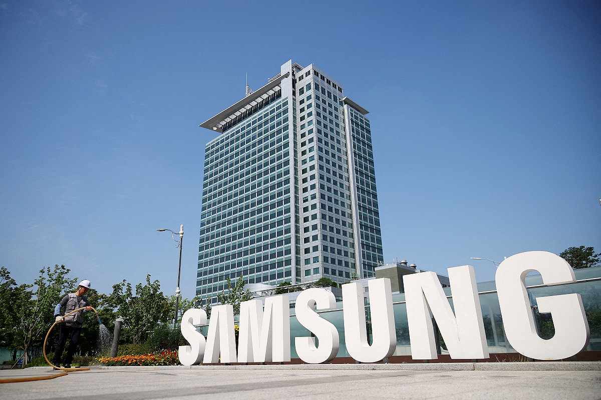
FILE PHOTO: A worker waters a flower bed next to the logo of Samsung Electronics during a media tour at Samsung Electronics’ headquarters in Suwon, South Korea, June 13, 2023.
14:12 JST, December 21, 2023
TOKYO/SEOUL, Dec 21 (Reuters) – South Korea’s Samsung Electronics 005930.KS will invest around 40 billion yen ($280 million) over five years in a facility for research into advanced chip packaging it will set up in Japan, according to an announcement by the city of Yokohama.
Reuters reported in March that Samsung was looking at establishing a packaging facility in Kanagawa prefecture, where it already has a research and development center, to deepen ties with Japanese makers of chipmaking equipment and materials.
The investment comes at a time of easing tensions between South Korea and Japan as the United States encourages allies to work together to counter China’s growing technological prowess.
Companies are racing to develop advanced packaging techniques, which involve combining components in a single package to improve overall chip performance.
The Japanese facility will allow Samsung to strengthen its leadership in chips and partner with packaging-related companies based in Yokohama, the head of Samsung’s chip business Kyung Kye-hyun said in the city’s announcement.
($1 = 142.8900 yen)
Most Read
Popular articles in the past 24 hours
-
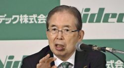
Nidec Chairman Resigns Amid Accounting Scandal at Major Japanese ...
-
Trump’s Address: Confront the Dead End that Authoritarianism Has ...
-
Humbert Humbert: Husband-Wife Vocal Duo Brings Cheerful Singing t...
-

Japan’s Hikonyan Cat Mascot to Celebrate 20th Birthday with Party...
-

Pakistan, Afghan Forces Clash after Days of Hostilities
-
Japan's Kairos Rocket Set to Launch on Sunday After Delays
-

China-linked Actor Tried Using ChatGPT to Target Japan's PM Takai...
-
JR Kyushu Mulls Using Trains for Concertgoer Lodgings; Performanc...
Popular articles in the past week
-
Producer Behind Pop Group XG Arrested for Cocaine Possession
-

Tokyo Skytree's Elevator Stops, Trapping 20 People; All Rescued (...
-

Nepal Bus Crash Kills 19 People, Injures 25 Including One Japanes...
-
Milano Cortina 2026: Japanese Gold Medalist Figure Skater Miura S...
-

Japan’s Major Real Estate Firms Expanding Overseas Businesses to ...
-

Reciprocal Tariffs Ruled Illegal: Judiciary Would Not Tolerate Pr...
-
Japanese High School Student Aims to Share Kaiten History Through...
-

Milano Cortina 2026: Miura-Kihara Duo, Other Japanese Figure Skat...
Popular articles in the past month
-
Producer Behind Pop Group XG Arrested for Cocaine Possession
-
Japan PM Takaichi’s Cabinet Resigns en Masse
-
Man Infected with Measles Reportedly Dined at Restaurant in Tokyo...
-

Israeli Ambassador to Japan Speaks about Japan’s Role in the Reco...
-
Videos Plagiarized, Reposted with False Subtitles Claiming ‘Ryuky...
-

Man Infected with Measles May Have Come in Contact with Many Peop...
-
Prudential Life Insurance Plans to Fully Compensate for Damages C...
-
Woman with Measles Visited Hospital in Tokyo Multiple Times Befor...
Top Articles in News Services
-
Survey Shows False Election Info Perceived as True
-
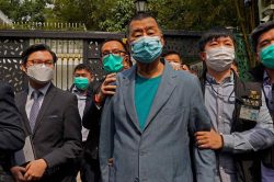
Hong Kong Ex-Publisher Jimmy Lai’s Sentence Raises International Outcry as China Defends It
-
Japan’s Nikkei Stock Average Touches 58,000 as Yen, Jgbs Rally on Election Fallout (UPDATE 1)
-
Japan’s Nikkei Stock Average Falls as US-Iran Tensions Unsettle Investors (UPDATE 1)
-
Japan’s Nikkei Stock Average Rises on Tech Rally and Takaichi’s Spending Hopes (UPDATE 1)
JN ACCESS RANKING
-
Producer Behind Pop Group XG Arrested for Cocaine Possession
-
Japan PM Takaichi’s Cabinet Resigns en Masse
-
Man Infected with Measles Reportedly Dined at Restaurant in Tokyo Station
-
Israeli Ambassador to Japan Speaks about Japan’s Role in the Reconstruction of Gaza
-
Videos Plagiarized, Reposted with False Subtitles Claiming ‘Ryukyu Belongs to China’; Anti-China False Information Also Posted in Japan